Laser Cutter For Silicon Wafer
Silicon Wafer Cutting Microholes Laser Drill Silicon Cutter

Micromachining A Silicon Wafer Laser Impressions Inc

Trial To Cut Silicon Wafer With Laser Cutter Youtube
Laser Dicing Technique Cuts Wafers From The Inside Out Features Jan 2008 Photonics Spectra

27 Laser Cut In Silicon Wafer Using 1064 Nm Wavelength Download Scientific Diagram

Silicon Wafers Laser Micromachining Silicon Wafer Cutting

Solutions are available for machining smaller diameter wafers from larger ones solar cell downsizing or silicon stencil cutting.
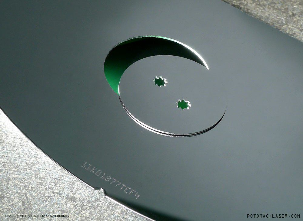
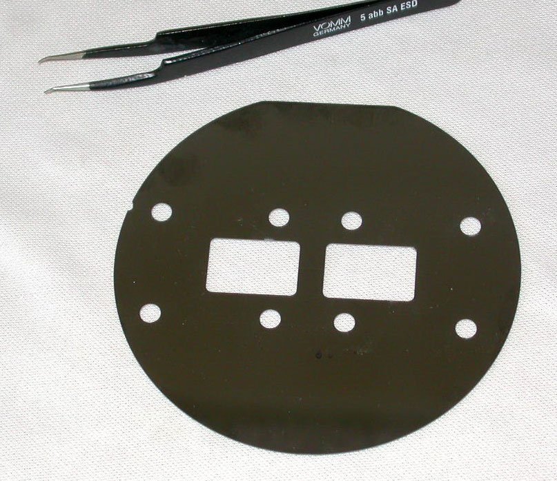
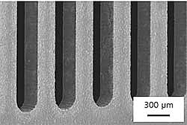
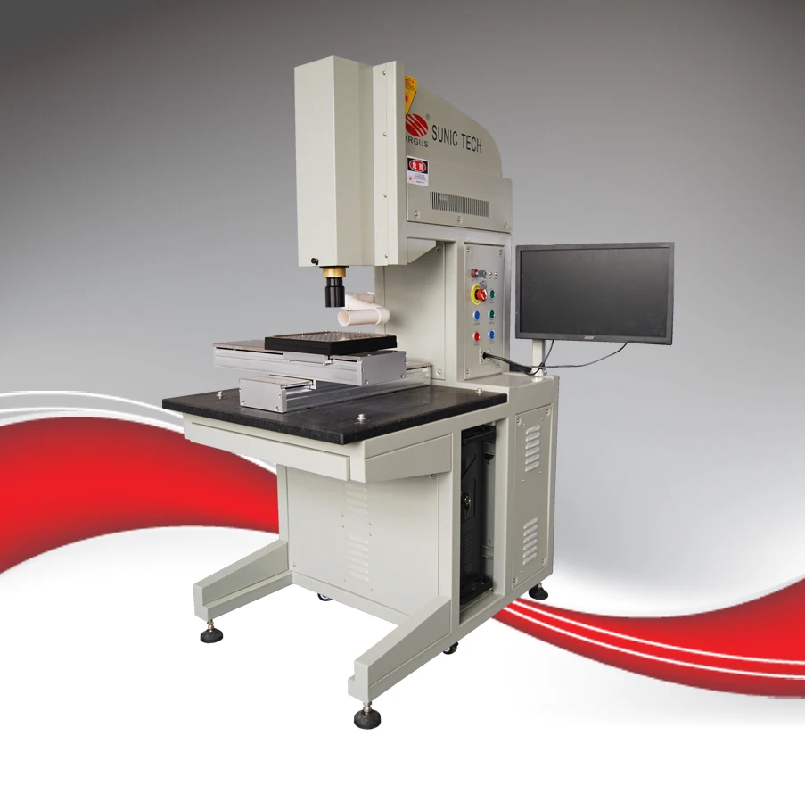
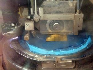
Laser cutter for silicon wafer. We tried cutting a silicon wafer with fabool laser mini 1 6w and 3 5w model. For silicon wafers less than 100 μm thick laser ablation offers an alternative to the blade technique which is too powerful for the delicate thin wafers. Laser cutting of silicon wafers is possible in all sizes and thicknesses with feature sizes as small as 20 microns. Demonstration of cutting features into 1 5 mm thick silicon wafers using a laser micromachining system equipped with a qcw laser.
Traditionally silicon wafers have been cut with diamond saws occasionally using a scribe and break process which have the limitation that they can only cut straight lines and suffer from edge chipping and frequency doubled vanadate lasers which are both slow and expensive to operate as is the microjet process. This is usually followed by a mechanical breaking procedure to produce silicon rectangular tiles for subsequent operations he mechanical break will follow allowing the scribing line offering the least path of resistance. Due to the reflection it only made slight scratch and could not cut. The same system can be used to downsize larger silicon wafers for use in smaller format processing tools.
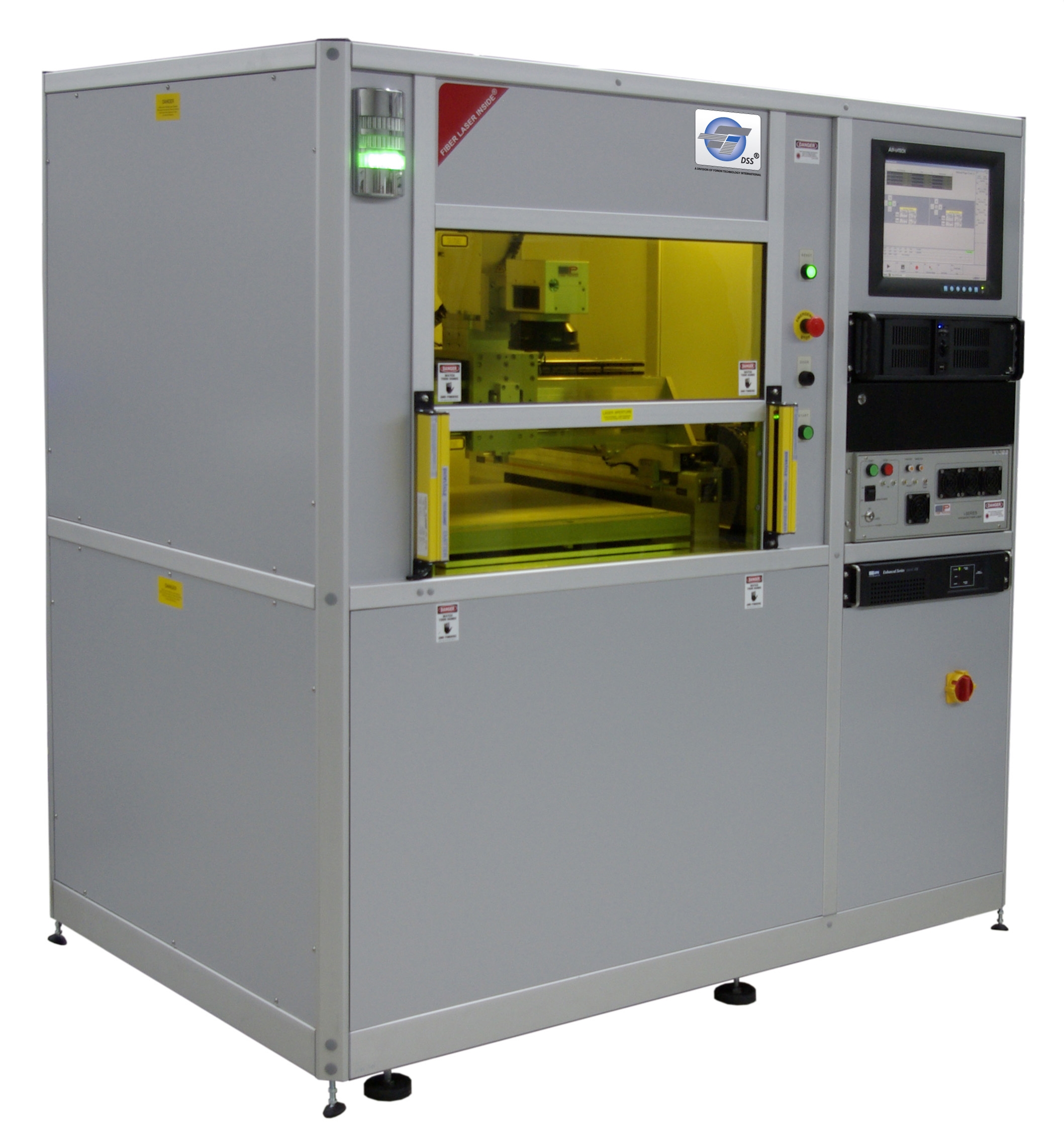
How is laser dicing silicon being processed. Material thickness up to 1mm. Laserod has a division that focuses on the building and integration of a full line of fiber laser micromachining equipment and a diode that can be used for laser dicing silicon wafer resistor trimming scribing substrates of silicon and alumina and cutting thin plastics and metals. In addition complex features such as channels and pockets and channels can be machined in silicon wafers.
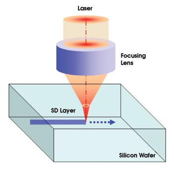
Dicing of silicon wafers may also be performed by a laser based technique the so called stealth dicing process. Sapphire silicon wafer cutter. The figure shows 700 µm wafer downsizing top view and side view. This lines introduces regions of weakness.
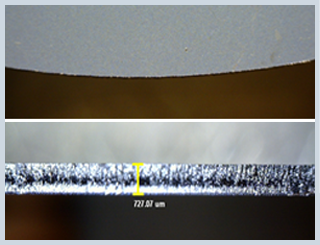
However laser ablation has its own problems. Cut features are round holes with no cracking or rough edges. It works as a two stage process in which defect regions are firstly introduced into the wafer by scanning the beam along intended cutting lines and secondly an underlying carrier membrane is expanded to induce fracture. Scribing causes partial cut lines on the wafer.

Cross Sections Of Silicon Wafers Cut By Different Techniques A By Download Scientific Diagram

Laser Cutting Silicon Wafers
Micro Laser Cutting Sapphire Diamond Ceramics Metals

Si Silicon Laser Processing Cutting Drilling
Scientist Manipulating Silicon Wafer During Laser Cutting Of The Same Stock Photo Alamy
Silicon Wafer Cutting
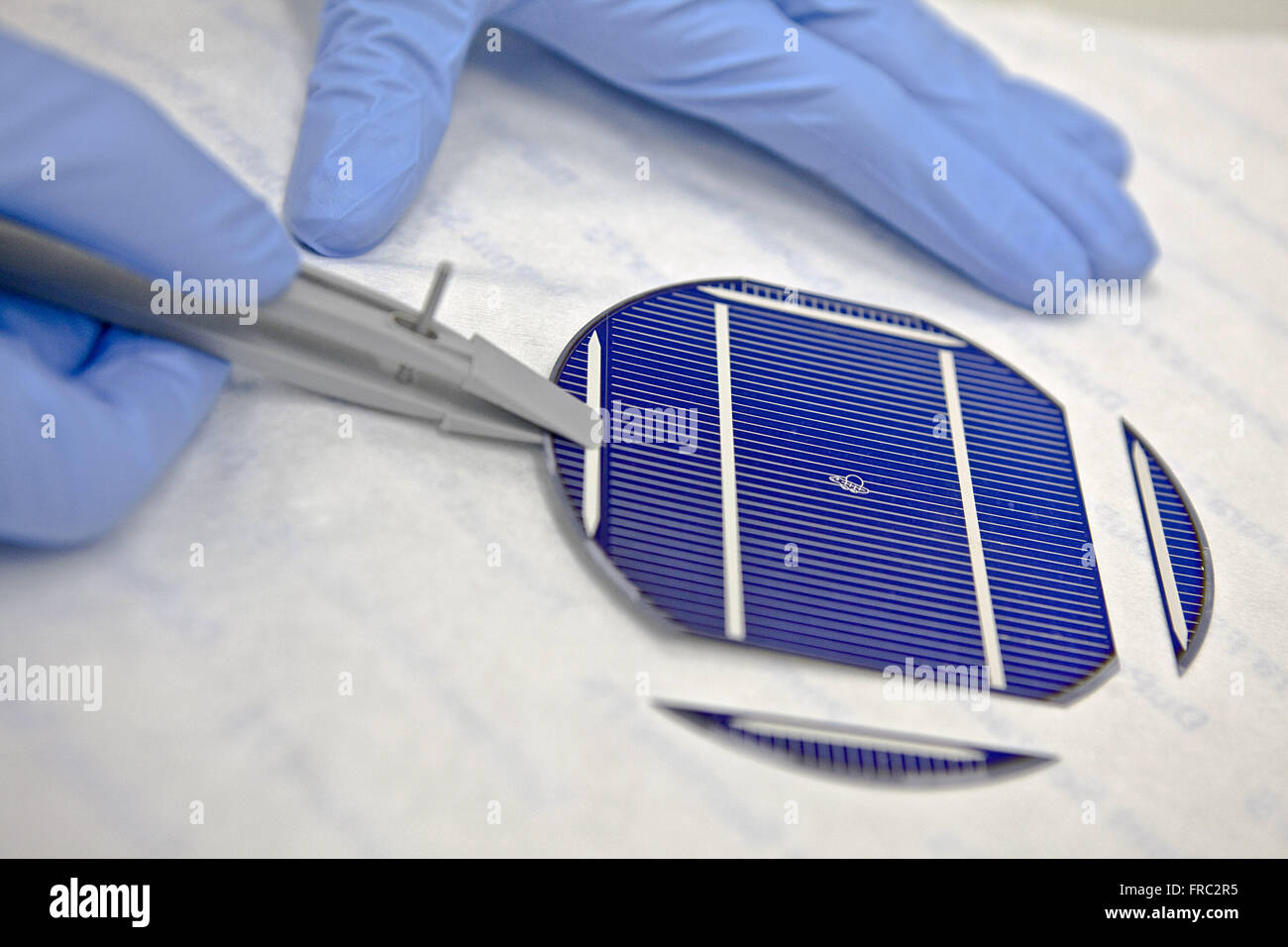
Laser Cutting Silicon Solar Cells

Wafer Resizing Coring Silicon Mems Laserod
Fiber Laser Cell Solar Silicon Wafers Scribing Cutting Dicing Easy Operation

Pre Crack Laser Thermal Cracking Method For Cutting Asymmetric Cutting Download Scientific Diagram

Fiber Laser Cutting Of Silicon Spi Lasers
China Silicon Wafer Cutting Machine Wafer Dicing Laser Scriber China Laser Cutter Fiber Cutter

Laser Dicing Wafer Cutting By Laser Microjet Ppt Video Online Download

Jg16b China Pico Laser Cutting System For Silicon Wafer Scribing Manufacturer Supplier
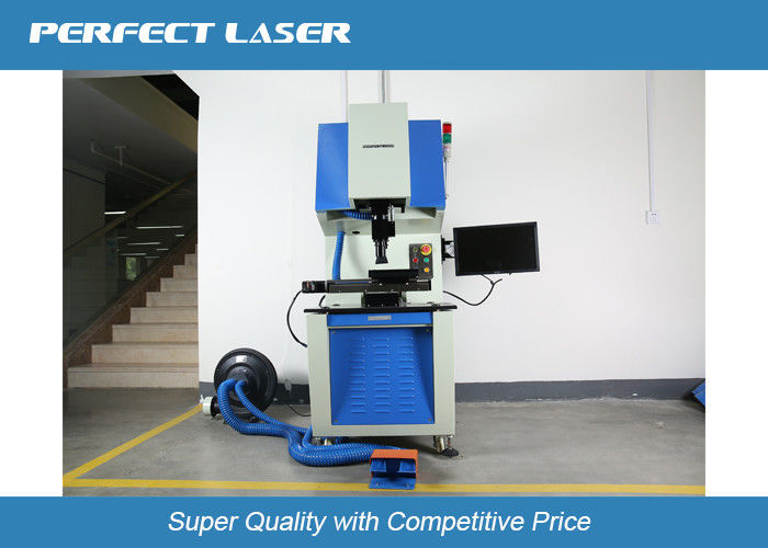
Perfect Laser High Quality Silicon Wafer Solar Cell Laser Cutting Dicing Scribing Machine Buy Laser Dicing Silicon Wafer Silicon Wafer Laser Scribing Machine Solar Cell Laser Scribing Machine Product On Alibaba Com

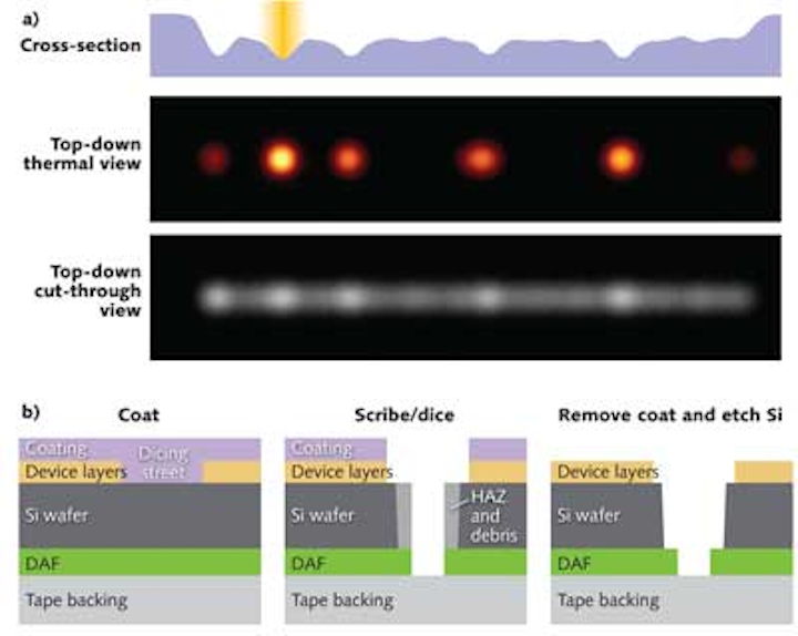
Multilayer Stack Materials On Silicon Based Wafer Dicing Processes Using Ultraviolet Laser Direct Dicing And Milling Methods Sciencedirect
Fine Laser Cutting Of Silicon Wafers Design For Laser Manufacture
Solar Cell Laser Cutting Machine Germany Ipg Silicon Wafer Solar Cells Scribing Cutting Machine Buy Ipg Solar Cell Laser Cutting Machine Silicon Wafer Laser Cutting Machine Solar Cell Cutting Scribing Machine Cutter Product On Alibaba Com
Leather Laser Cutting Machine Price Product Printer Laser Ltt Buy Leather Laser Cutting Machine Price Laser Product Laser Cut Printer Ltt Laser Product On Alibaba Com
Best Laser Cutting Drilling Experts Laserod By Laserod Wafer Medium

Wafer Alignment And Dicing Process A Silicon Wafer With Sputtered Download Scientific Diagram
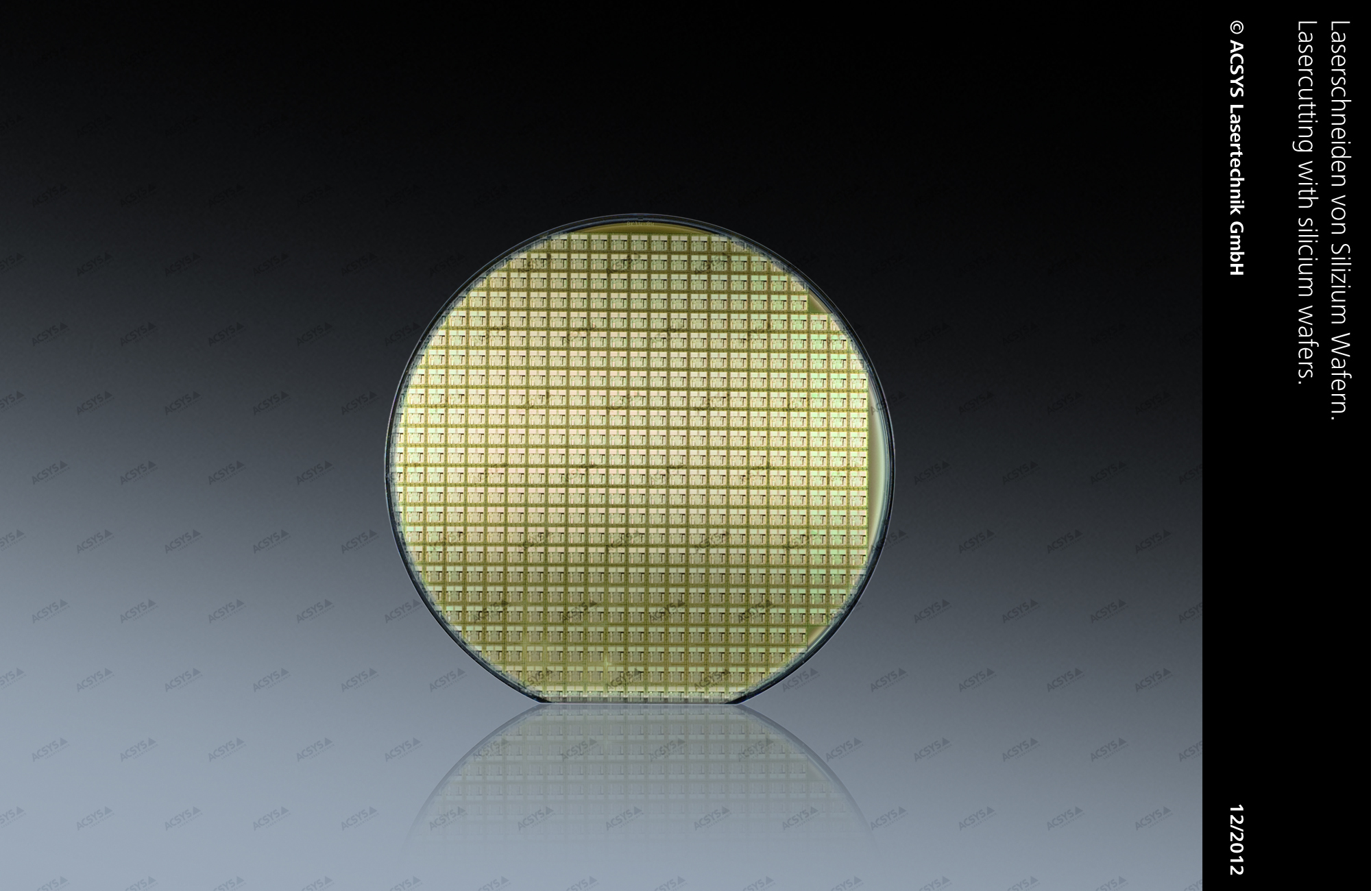
Applications Laser Cutting Acsys Lasermaschinen

China Keyland Pv Cell Manufacturing Solar Module Making Equipments Silicon Wafer Solar Cell Laser Cutting Machine China Solar Cell Laser Scribing Machine Solar Cell Cutting Machine

China Silicon Wafer Cutting Machine Solar Machine Cutting Solar Cells China Laser Cutter Fiber Cutter
Fiber Laser Cell Solar Silicon Wafers Scribing Cutting Dicing Easy Operation For Sale Laser Scribing Machine Manufacturer From China 106948302
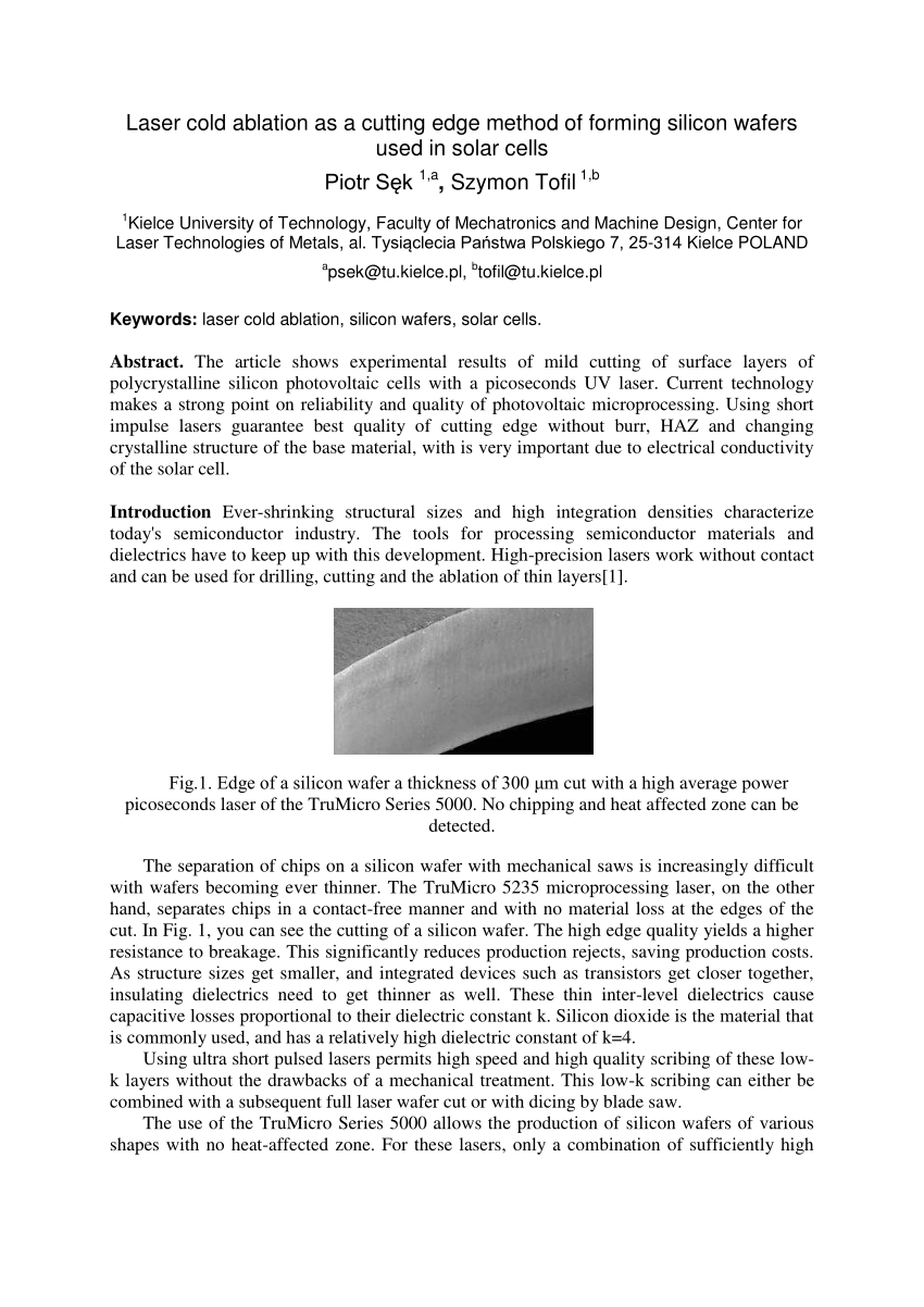
Pdf Laser Cold Ablation As A Cutting Edge Method Of Forming Silicon Wafers Used In Solar Cells
Microelectronics Processing Zero Overlap Laser System Speeds Ultrathin Wafer Dicing Laser Focus World

Laser Cutting Laser Engraving Machine Monocrystalline Silicon Solar Cell Laser Miscellaneous Wafer Solar Cell Png Pngwing

France Agent 100w 150w Mdf Plywood Wooden Perfect Laser 3d Surface Laser Engraving Machine Mdf Plywood Laser Engraving Machine Mini Laser Engraver
Pdf Laser Cutting Of Silicon Wafer By Pulsed Nd Yag Source

Laser Cutter Laser Cutter System Failure Analysis Design Validation 1064 Nm Wavelengths 532 Nm Wavelengths 355 Nm Wavelengths 266 Nm Wavelengths Lcd Materials Semiconductor Materials

Laser Cutting Stanford Nanofabrication Facility

China Zlh706 Laser Dicing Saw For Semiconductor Wafer Cutting China Laser Saw Wafer Laser Saw

China Silicon Wafers Fiber Laser Scriber Cutting Machine China Silicon Wafers Laser Scriber Machine Silicon Wafers Laser Cutting Machine
Silicon Wafer For Solar Cell Fiber Laser Scribing Machine Solar Cell Cutting Machine Fiber Laser Scriber Buy Fiber Laser Scribing Machine Solar Cell Fiber Laser Scibing Machine Silicon Wafer Solar Cell Fiber Laser

Process Window To Cut Silicon Wafer Materials Using A Laser Beam Of 2 Download Scientific Diagram
Silicon Machining Silicon Wafer Downsizing Questech Services Corporation
Silicon Wafer Cutting Boao Laser Fiber Laser Cutting Machine Price Metal Laser Cutting Machine

Pico Laser Cutting Company
Laser Dicing Silicon
Dicing Lnf Wiki

Brief Introduction Of Uv Laser Marking Machine Laser Engraver Forum

Crystal Glass Silicon Wafer Code Uv 355nm Laser Marking Machine For Sale Wood Routers Aliexpress

