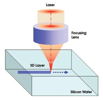
Laser Dicing Silicon Wafer
Laser Dicing Technique Cuts Wafers From The Inside Out Features Jan 2008 Photonics Spectra

Stealth Laser Dicing Youtube
.jpg)
Wafer Analysis Of Laser Grooving
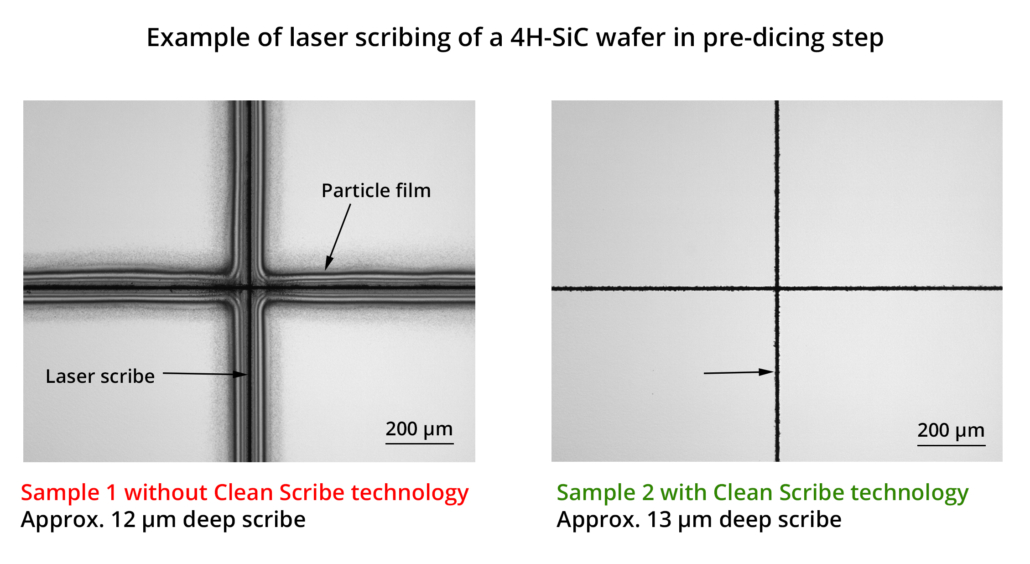
3d Micromac Unveils Clean Scribe Technology On Microdice Tls Laser Dicing System For Low Cost Particle Free Dicing Of Silicon Carbide Wafers Laser Micromachining 3d Micromac Ag

At Dsk Technologies Silicon Dummy Mechanical Grade Wafers Are Available In Sizes From 2 To 12 Diameter This Silicon Dummy Wafer Is Dummy Wafer Web Design

Silicon Wafer Dicing All Diameters 27 Years Of Experience Svm

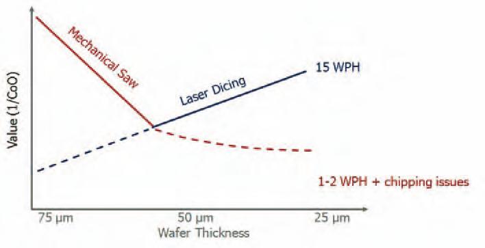
For silicon wafers less than 100 μm thick laser ablation offers an alternative to the blade technique which is too powerful for the delicate thin wafers.
Laser dicing silicon wafer. The same system can be used to downsize larger silicon wafers for use in smaller format processing tools. Silicon wafer dicing blackstar wafer dicing system blackstar is a wafer dicing system utilizing fantom width laser dicing technology fwldt invented and patented by laser photonics and modified to accommodate the requirements of a silicon wafer singulation process without affecting the existent dicing method processes or procedures. It works as a two stage process in which defect regions are firstly introduced into the wafer by scanning the beam along intended cutting lines and secondly an underlying carrier membrane is expanded to induce fracture. Laserod s production division specializes in high resolution small spot size laser machining and silicon wafer resizing for semiconductor medical solar and microelectronics applications as well as patterning for the display industry.
Blade dicing laser dicing and stealth dicing available on bare silicon patterned soi wafers and other non silicon materials. Svm wafer dicing capabilities. How is laser dicing silicon being processed. Vaporizing the wafer with a laser along the dicing path creates molten debris and microcracks.
The microdice laser micromachining system leverages tls dicing thermal laser separation a unique technology that uses thermally induced mechanical forces to separate brittle semiconductor materials such as silicon si silicon carbide sic germanium ge and gallium arsenide gaas into dies with outstanding edge quality while increasing manufacturing yield and throughput. Compared to dicing with a rotary saw or laser ablation the proposed method lowers equipment cost from more than 50 000 to 1 000 for silicon wafer dicing. The chapter provides an overview about the laser dicing process of electronics substrates with the focus on silicon. Patterned and non patterned wafer substrates.
Cut features are round holes with no cracking or rough edges. Laserod is a pioneer in maskless fast prototyping of laser patterns on a broad variety of substrates. The minimum die dimension that the proposed method can achieve is 3 mm by 3 mm which in most cases meets the fabrication requirement of microfluidic chips. We specialize in processing very thin substrates with.
However laser ablation has its own problems. Compared to industrial processes mechanical or already laser based dicing with ultra fast lasers promises material removal without damaging or weakening the surrounding material around the cut. Laserod has a division that focuses on the building and integration of a full line of fiber laser micromachining equipment and a diode that can be used for laser dicing silicon wafer resistor trimming scribing substrates of silicon and alumina and cutting thin plastics and metals.

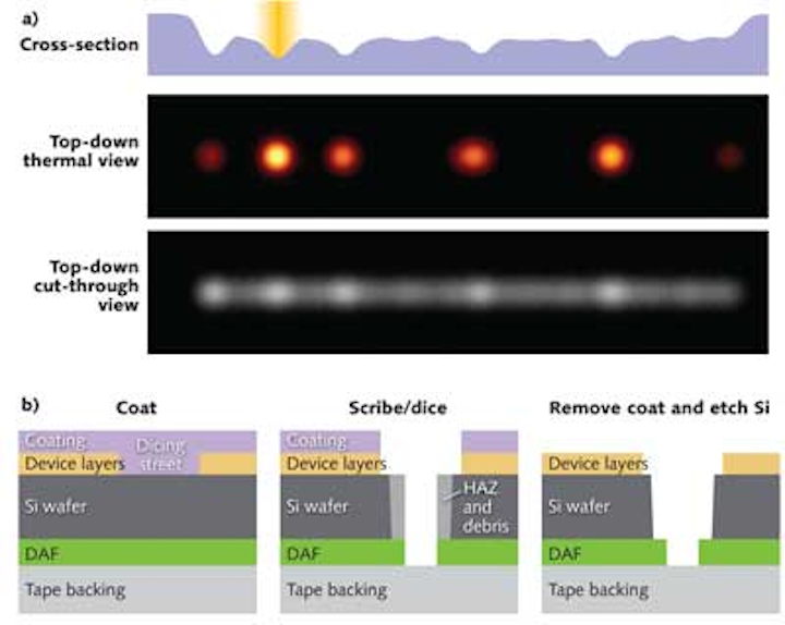
Multilayer Stack Materials On Silicon Based Wafer Dicing Processes Using Ultraviolet Laser Direct Dicing And Milling Methods Sciencedirect
Microelectronics Processing Zero Overlap Laser System Speeds Ultrathin Wafer Dicing Laser Focus World

Laser Dicing Wafer Cutting By Laser Microjet Ppt Video Online Download

Wafer Resizing Coring Mems Laser Marking Laser Machine

Laser Process Wafer Wafer Marking Wafer Dicing Wafer Cutting Wafer Scribe Youtube

Chuck Table Chucks Ceramics Black And Brown

Dsk Technologies What Matters Is Choosing The Right Companies Like Dsk Technologies For Picking The Right Electronic Parts The Co In 2020 Tape Wafer Electronic Parts
Laser Dicing Silicon

Laser Processing Of Doped Silicon Wafer By The Stealth Dicing Semantic Scholar

Mold Cleaning Rubber Sheet Looking For An Efficient Solution For Mold Sheet Cleaning Read Here For The Dsk Technologies With Images Mold Release Molding Led Manufacturers

Silicon Mems Micromachining And Patterning Mems Laser Machine Detector

Semiconductor Production Support With Fiber Lasers Spi Lasers

Trial To Cut Silicon Wafer With Laser Cutter Youtube

Laser Dicing Silicon

For System Integration And Shop Service Laser Resistor Trimming Of Thick And Thin Film Hybrid Microelectronic Devices Active An Resistors Thin Film Graphing

Microdice Wafer Dicing System For Sic Youtube

Silicon Wafers Producers And Suppliers Company Semiconductor Materials Wafer Semiconductor
Laser Scribing Sapphire Silicon Carbide Wafer Scribing
1
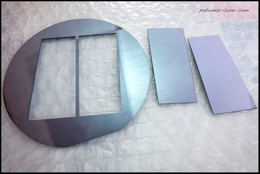
Rapid Dicing Of Silicon Wafers Potomac Photonics Fablab Examples

Figure 3 From Uv Laser Dicing Without Failure Caused By Contamination And Heat For Thick Anodically Bonded Silicon Glass Mems Wafers Semantic Scholar

The Mechanism Of Wafer Dicing Process The Water Jet Guides The Laser Download Scientific Diagram

Figure 1 From Uv Laser Dicing Without Failure Caused By Contamination And Heat For Thick Anodically Bonded Silicon Glass Mems Wafers Semantic Scholar
Laser Dicing Solutions Disco Laser Features Advantages Disco Corporation

High Speed Laser Wafer Scribing Industrial Laser Solutions

Pdf Assessment Of A Lasersingulation Process For Si Wafers With Metallized Back Side And Small Die Size Stephan Schoenfelder Academia Edu

Pdf Ultrafast Laser Dicing Of Thin Silicon Wafers Strategies To Improve Front And Backside Breaking Strength

Laser Beam Induced Thermal Crack Propagation For Asymmetric Linear Cutting Of Silicon Wafer Sciencedirect
Semiconductor Dicing Tapes Laser Dicing
Https Www Spiedigitallibrary Org Proceedings Download Fulldoi 10 1117 2f12 2289235

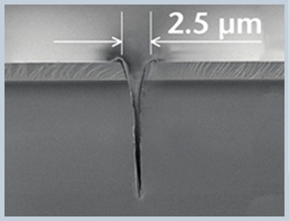
Figure 3 From Multi Beam Laser Grooving Process Parameter Development And Die Strength Characterization For 40nm Node Low K Ulk Wafer Semantic Scholar
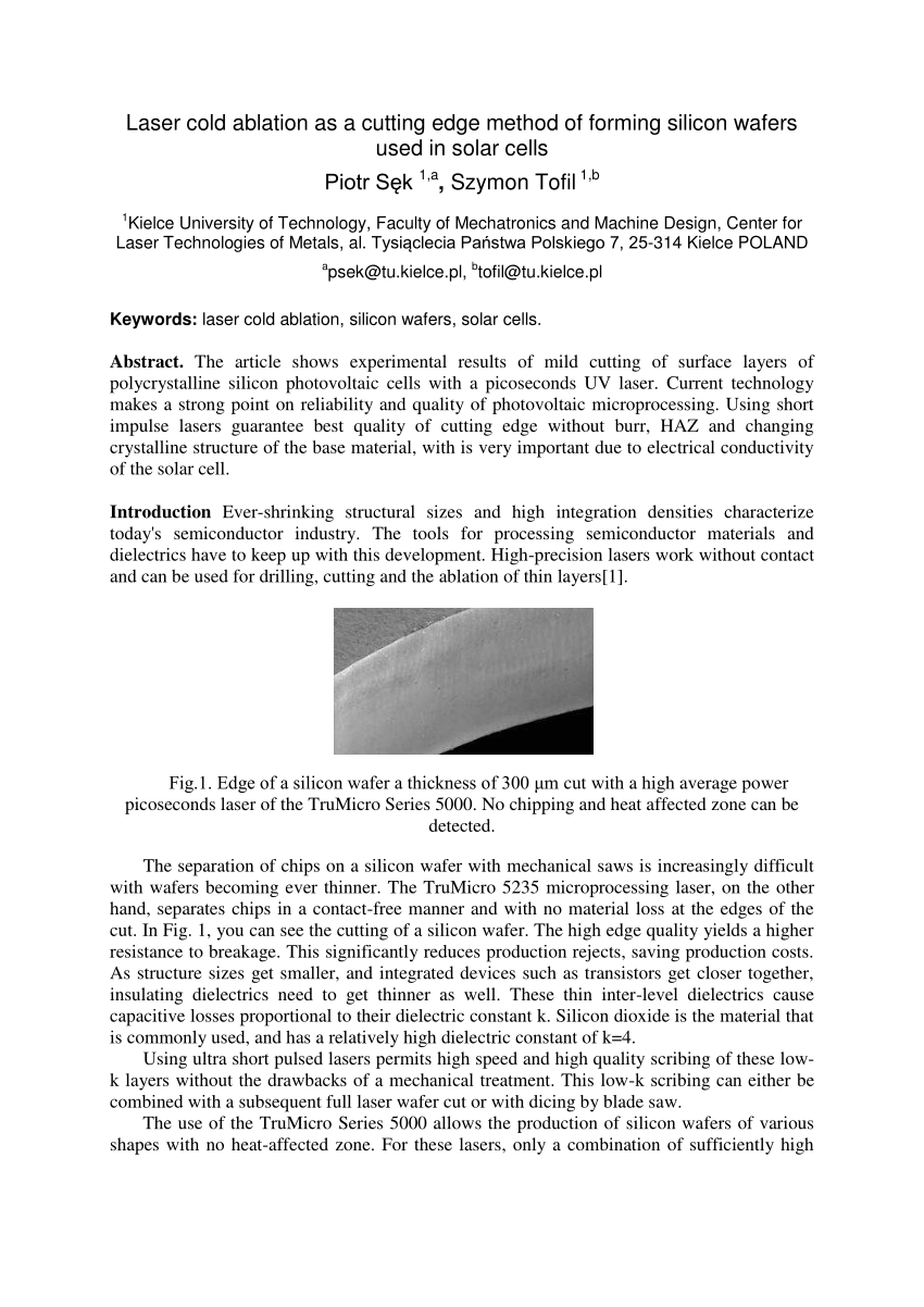
Pdf Laser Cold Ablation As A Cutting Edge Method Of Forming Silicon Wafers Used In Solar Cells

Applications Next Scan Technology Technology Scanner Scan

Uv Dicing Tape Wafer Dicing Surfactant Mold Release Film Silicon Dummy Wafer Wafer Dicing Tape Uv Dicing Tape In 2020 Mold Release Cleaning Mold Led Manufacturers
Polysilicon Wafer Photovoltaic Wafer Silicon Laser Wafer Dicing Machine 350mm 20w Buy Laser Wafer Dicing Machine Laser Fiber Silicon Wafer Dicing Machine Laser Dicing Laser Scribing For Silicon Wafer 20w Product On Alibaba Com
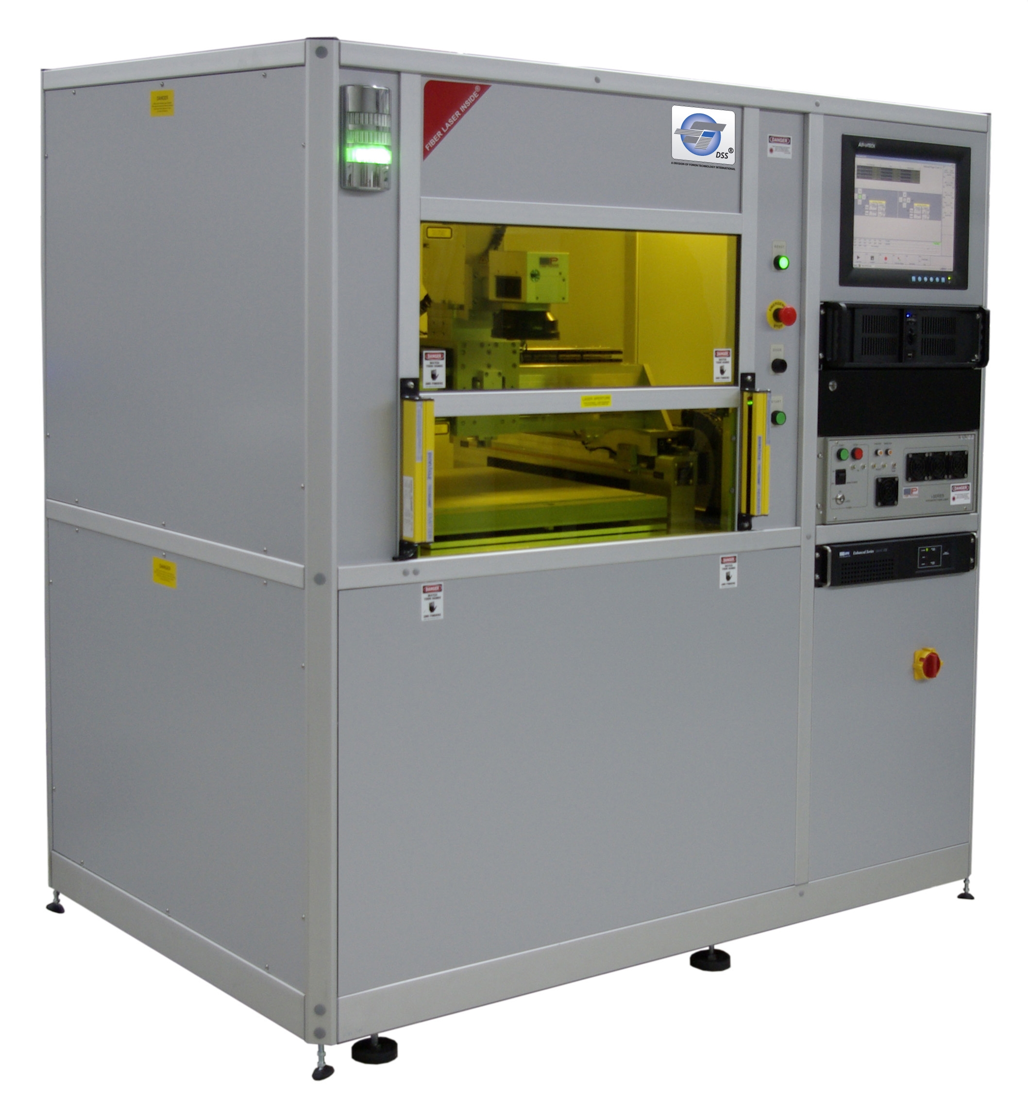
Silicon Wafer Dicing Blackstar Sw300

Laserod Has Been Enjoying Some Success In Laser Machining Of Mems Devices Mems Are Microelectromechanicalsystems Moems Are Optical Laser Machine Microelectromechanical Systems

Mold Cleaning Rubber Sheet Looking For An Efficient Solution For Mold Sheet Cleaning Read Here For The Dsk Technologies With Images Mold Release Molding Led Manufacturers
Pdf A High Repetition Rate Femtosecond Laser For Thin Silicon Wafer Dicing
Http Ewh Ieee Org Soc Cpmt Presentations Cpmt1709a Pdf
Https Www Spiedigitallibrary Org Conference Proceedings Of Spie 10520 105200d Direct Observation Of Internal Void Formation In Stealth Dicing 10 1117 12 2288238 Pdf

China Silicon Wafer Cutting Machine Wafer Dicing Laser Scriber China Laser Cutter Fiber Cutter

Semiconductor Control Micro Systems

